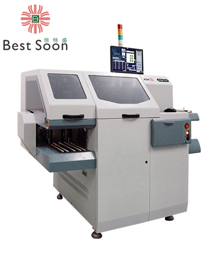

AD830P-Plus ASMPT Automatic Die Bonder
Feature
●High-speed, high-precision die bonding
●Polycrystalline LED processing capability
●Top-view lens to identify the PN electrode at the bottom of the chip
●Poly crystal arm module (option)
●Brand new image recognition system
●At the time of glue dispensing and die bonding, image recognition and inspection are carried out at the same time to improve production efficiency
●"PR On The Fly" top-view image recognition capability, which can improve the precision of die bonding position without losing the die bonding cycle time
●Option: Downward-looking lens for double-sided image inspection of the chip
●Realize factory automation
●Fully automatic material handling capability
●Fully automatic wafer handling system (option)
●Connectivity (option)
Size
Width, depth and height
1,740 x 1,240 x 2,080mm