ASM’s packaging technology is the future of high-power electronics, and traffic is one of the world’s biggest sources of air pollution, accounting for one-fifth of global carbon emissions and rising. In order to drive vehicles, human beings consume a lot of fossil fuels, such as gasoline, diesel oil or LPG, which produce a lot of pollutants such as carbon monoxide, carbon dioxide, nitrogen dioxide and so on, which cause serious air pollution, all of these substances are harmful to human health. To improve air quality and combat air pollution, clean energy has been actively promoted around the world in recent years to gradually replace fossil fuel technology to reduce carbon emissions and combat warming. These alternatives are Electric, including Battery Electric Vehicle (Bev) or Plug-in Hybrid Electric Vehicle (Phev) configurations. This wave of car electrification requires automakers to use a lot of semiconductor technology in their solutions, as well as to design and assemble more High-power erd Electronics (HPE) to drive future car development. In a classic line from a Superhero Movie, “The more power, the more heat”! For high-power electronic components of the HPE class of electric vehicles, the operating conditions may be very harsh, as the temperature of ordinary vehicles is usually over 150 degrees Celsius. In order to protect these carefully designed and assembled components and enable them to continue to generate high voltages and currents to power and operate vehicles at such high temperatures, advanced packaging technology is key.
UNDERSTANDING HIGH-PERFORMANCE PACKAGING: The power package behind a high-power electronic component in an electric vehicle system consists essentially of a generator, motor, inverter, battery, battery charger, and Electrical Control Unit (Ecu) . The ECU is the location of high power electronic components such as Double-Sided Cooling Package (DSC) and Single-Sided Cooling (SSC) . In order to protect DSC and SSC packages, manufacturers usually use a transfer molding process using silver paste. Figure 1A shows a typical DSC internal structure with a top lead frame and a bottom Direct Copper Bond (DBC) for dissipating the heat generated while providing high voltage and current levels. In order to completely eliminate the large amount of heat generated, DSC is integrated into the cooling system in a mechatronics engineering manner, acting as a radiator to dissipate heat for the components in operation.
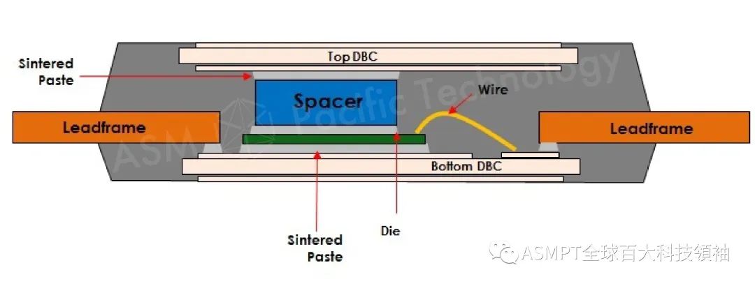
FIGURE 1A: In contrast to the SSC in figure 1B, the double-sided cooling (DSC) module schematic shown in figure 1A shows that the SSC is usually connected to a pin-fin module to dissipate the heat generated.
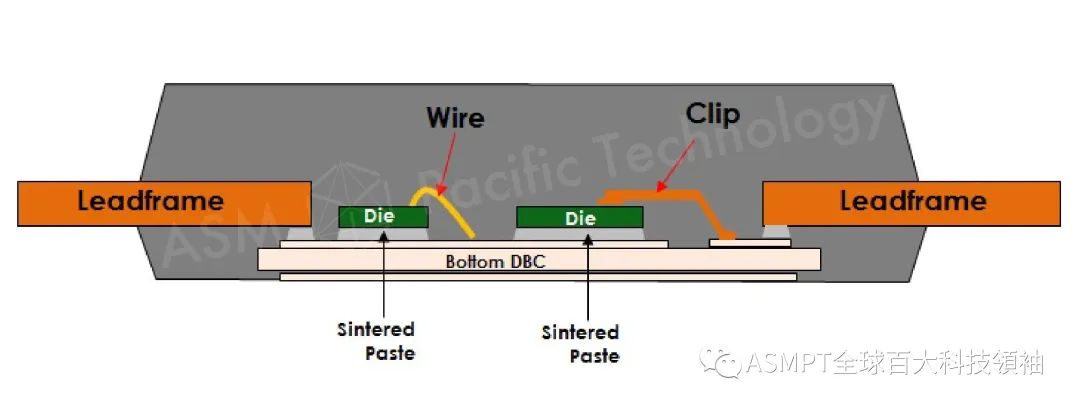
FIGURE 1B: Schematic Diagram of a single-side cooling (SSC) component, whether DSC or SSC, presents multiple challenges in its modeling. The first is Mold Bleed and Flash (MBF) or chip cracking, both of which can cause component damage and reduce solderability. Another potential problem is layering and voids, which usually occur during design and setup due to the use of suboptimal processes and processes. In response to the challenge, such defects and defects will affect the quality of high-power electronic components HPE, especially in the production of high-quality HPE for automotive use more need to avoid defects. Usually these problems can be solved in four main areas: indirect materials, process setup, incoming materials, and tool design (see figures 2 and 3) . For the purpose of this paper, emphasis will be placed on MBF and chip crack, which are common problems in the current Z process. In the mind map in figure 2, one of the significant causes of Wafer Crack Z is the nature of incoming material. To solve this problem, manufacturers need to exercise strict quality control when purchasing materials from third parties, such as paying attention to the dimensional quality of DBC substrates. Subsequent challenges related to wafer integrity, including dimensional accuracy of wafer placement, coplanarity of solid-state crystals, and wafer centering over silver.
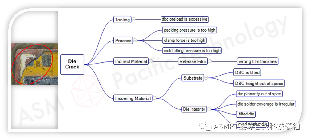
Figure 2: Mind Map of Wafer crack. In figure 3, the main cause of MBF is the penetration of Epoxy molding Compound into the top and bottom of DBC exposed pads. This problem is attributed to the mold design. This is consistent with Asm Pacific Technology’s years of design and research experience in the field.
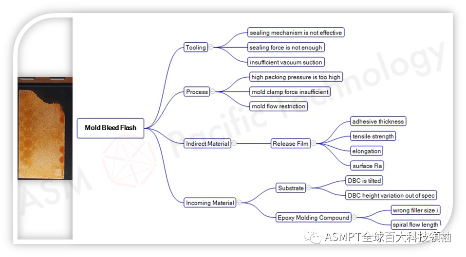
Figure 3: Mind Map of the die exhaust flash (MBF) figure 4 shows a diagram of the ideal molding process, where the molding tool is designed to have a good sealing ability.
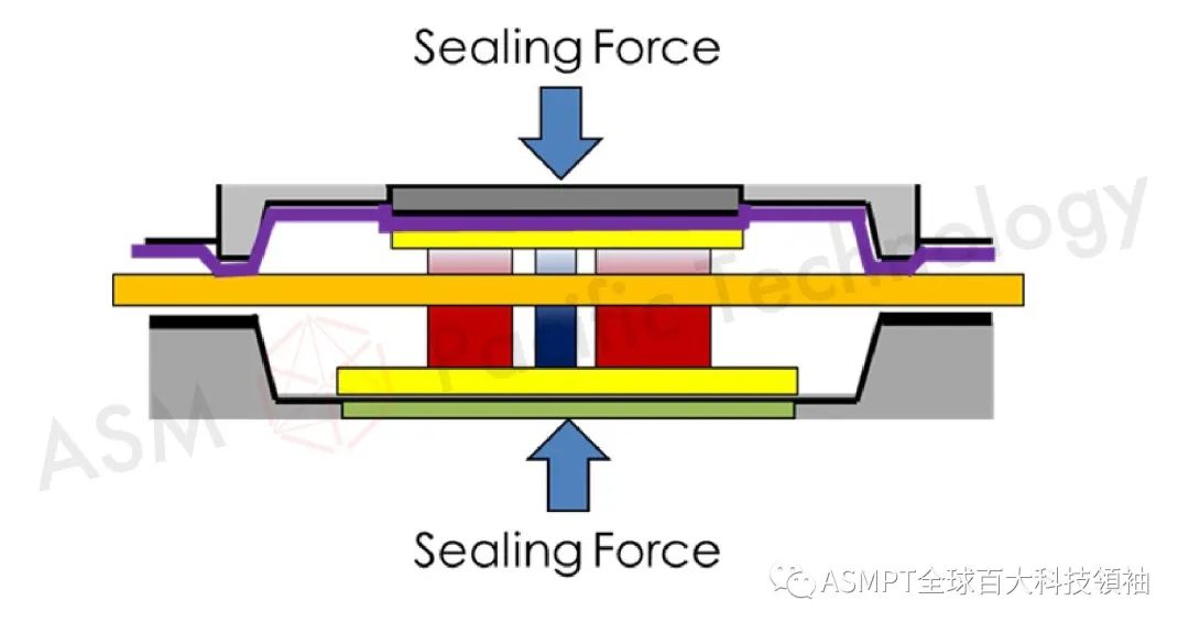
Figure 4: Seal of MBF control device. In summary, many key factors need to be solved first to produce high quality HPE and package structure, two of which are chip crack and MBF, factors leading to these problems include incoming materials, mold accuracy and mold design. Advanced packaging Technology from ASM Pacific Technology, along with years of research expertise in the field, will help meet all packaging needs.