ASM solid crystal machine Micro LED mass transfer technology schools and process analysis Micro display in recent years, Micro LED due to its low power consumption, fast response, long life, high light efficiency, etc. , it is seen as the next generation of display panel technology after LCD and OLED. Micro Light Emitting Diode, also known as μLED in Chinese, is a thin film, miniaturization and Matrix of traditional leds that reduces pixel distance from millimeters to microns, and a highly integrated solid-state self-luminescent display on a chip, which differs from conventional leds in size, is about 1/10th the size of a human hair and 1% the volume of a mainstream LED, however, there is no uniform definition of Pixel size. Micro LED micron-scale Pixel spacing allows it to cover from small and medium-sized display to large and medium-sized display and other applications. Compared with the traditional small-pitch LED, the display resolution and picture quality are greatly improved due to the miniaturization. The optical design can make the visual angle wider, the contrast higher, the picture quality better, suitable for the virtual reality, the small projector, the micro display, visible Light Communication, medical research, and more. Compared with Oleds, they all display with self-emitting technology, allowing integrated sensors and circuits to realize the embedded sensing function, and flexible display with flexible substrate, it can be used in flexible display fields such as wearable/implantable devices and on-board display. In addition, Micro leds have high definition, high brightness and good contrast, high response speed is very suitable for VR, AR and other wearable devices that require high response speed (high brightness and energy saving for outdoor wear occasions) .
The concept of Micro LED displays didn’t come to commercial attention until 2012, when Sony showed off a crystal-LED microLED TV, different research institutions and companies have begun to focus on such bottleneck technologies as microfabrication, full color process, and wafer transfer. According to the different sizes of display panels used in different applications, the fabrication of displays can be divided into single-chip manufacturing technology and mass transfer technology, single-chip manufacturing (SCM) technology is to fabricate high-resolution display directly on Si, Gan or Sapphire substrates by Micro-LED, and then peel off the substrate by physical or chemical mechanism. This approach avoids the complicated mass transfer process, but is limited to building smaller displays, such as near eye displays and smartwatches, limiting the application scenarios for Micro leds, each process can only grow on the substrate of a color light bead chip, so this single-chip manufacturing technology can not solve RGB full-color display. In recent years, quantum dots full-color displays have been proposed, in which the light emitted by a single ultraviolet Micro LED is used to excite the red, green and blue light-emitting media covered on top of the Micro LED, thus achieving full-color display, this colorization alternative technology in the future development may fill the single-chip manufacturing in full-color limitations. Another manufacturing technique is mass transfer, in which LED wafers are grown on the source substrate and then separated from the source substrate and transferred to the display electronic device quickly, accurately and reliably by some force.For a wider range of display applications such as mobile phones, tablets and televisions, the substrate is separated from the substrate after fabrication, it is inevitable that Micro LED chips will be assembled on a larger size substrate with logic circuit by means of mass transfer to meet the application requirements. In addition, flexible and stretchable optoelectronic devices for wearable and bioelectronic applications have recently gained wide popularity. These applications require the transfer of leds to flexible substrates, as well as a huge amount of transfer. However, because the size of each transfer chip is very small and the quantity is very large, the accuracy and speed of transfer process is very high, which has become the key technology to limit the mass production of Micro LED. In this paper, the Micro LED mass transfer technology is briefly introduced, and the difficulties and challenges in this technology are analyzed. According to the process of in-process technology, the mass transfer process can be divided into two key processes: substrate separation and wafer transfer. The principle, research progress and key research issues of each process are described respectively, then, the development prospect of mass transfer technology is prospected.
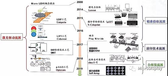
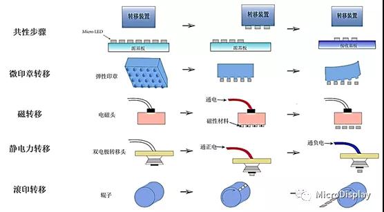
1. Because of the smaller size of the LED chip to be transferred, it is about 1/10 of the hair, so it needs high precision and fine operation A transfer needs to move tens of thousands or even more than one hundred thousand LED, the number is very huge, requires a very high transfer rate, the traditional LED chip in the packaging, mainly using vacuum absorption way, the physical limit of the vacuum tube is only about 80 μm, while the Micro LED size is below 50 μm THE PRECISION OF CURRENT PICK & Place is ± 34 ΜM (Multi-Chip Transfer) and Flip Chip Bonder is ± 1.5 μm (single Chip per Transfer) . It can be seen that the traditional wafer transfer technology can not transfer millions of wafer table 1 with micron size in an economical and high precision way. In order to solve these problems, many companies and research institutions have carried out a lot of research based on different principles and formed an accurate pick-up. Chart 2 of ASM solid crystal machine huge mass transfer mainstream technology development.The precision pick-up genre technology is mainly different from the transfer head adsorption LED force. Luxvue uses a dual-electrode transfer head to transfer the wafer from the source substrate to the target substrate via electrostatic pickup and placement. X-Celeprint uses an elastic seal as the transfer head to pick up the wafer using Van der Waals force, and then placed on the target substrate, with the development of technology, huge transfer is no longer limited to the traditional pick-up process, laser-driven transfer technology has been applied in the transfer, to non-contact processing technology, bulk parallel transfer UNIQARTA, Coherent, QMAT uses laser-induced forward transfer (LIFT) process to separate wafers by laser-material interaction, the resulting local impact forces propel the wafer toward the substrate. OPTOVATE proposes a p-LLO process, in which Gan is split into nitrogen and liquid Ga by laser action for stripping and transfer. In addition, Elux and Self array adopt Self-assembly technology, which is based on fluid Self-assembly and magnetic Self-assembly respectively. The Korea Institute of Machinery and materials (KIMM) put forward the transfer technology of self-alignment roll printing, which can realize huge transfer by roll printing. The current technology has made some progress based on different principles of action, but there are still some problems such as yield, precision and transfer rate. How to control the cost and yield has become the key to commercialization. Mass transfer technology is divided into two key processes: (1) substrate separation: the substrate is separated from the source substrate by a certain force; (2) Wafer pickup and placement: the separated Micro LED chip is selectively picked up from the source substrate and transferred to a specific position of the target display substrate by a transfer device.
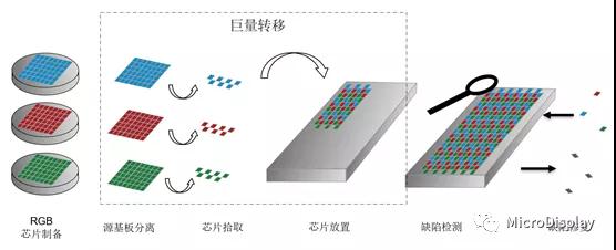
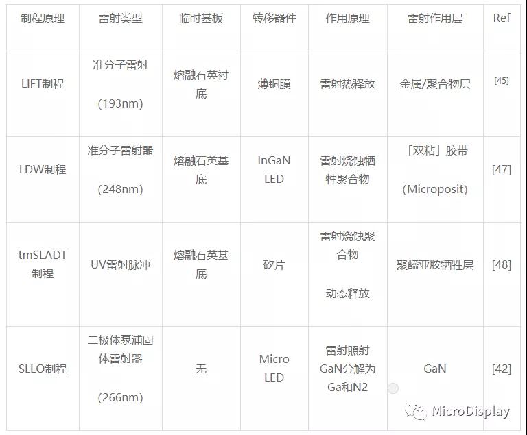
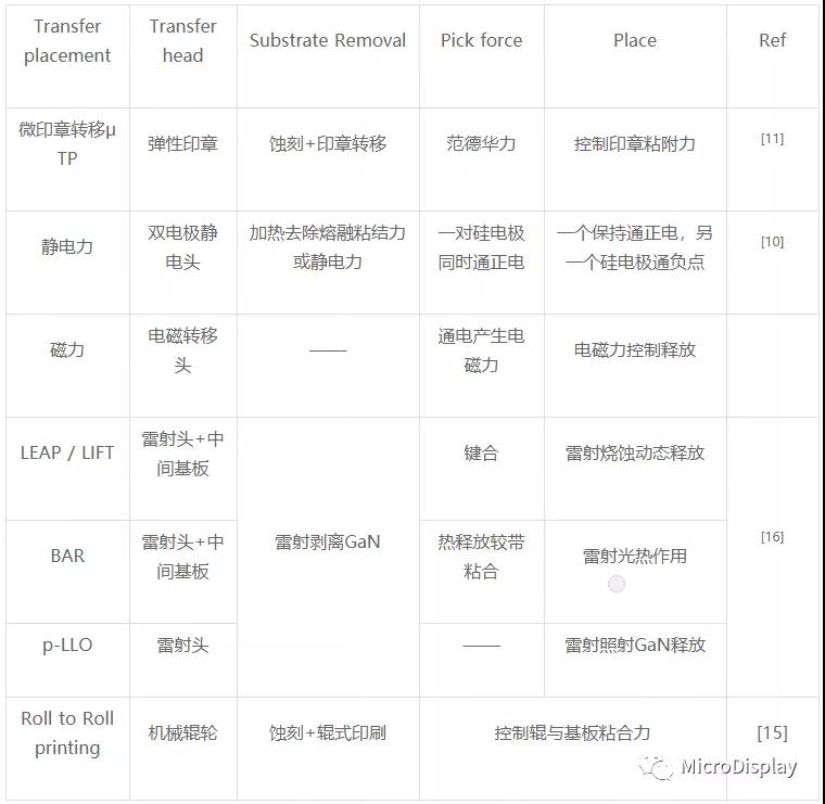
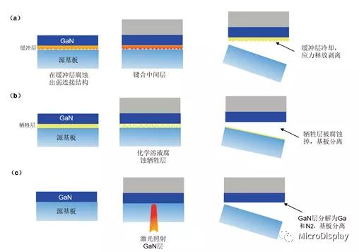
ASM SOLID-CRYSTAL MACHINE FIGURE 3 mass transfer technology flow, however, due to the transfer of Micro LED size compared to the mainstream chip size smaller, more integration, the traditional LED substrate stripping, transfer technology such as mechanical ejector pin, vacuum adsorption pick-up process window is greatly reduced, the technical and cost requirements are higher, there are still yield, accuracy and other problems, how to control the cost and yield has become the key to commercialization. Table 2 lists the substrate separation techniques and pick-up forces in different schools of mega transfer technology. Table 2 principle of huge mass transfer technology ASM solid crystal machine 2. Micro leds are usually grown on SI and Sapphire substrates to form Gan epitaxial layers. In order to reduce the limitation of wafer size and extend to medium and large size display and flexible display, substrate removal technology is needed to peel off the source substrate, current substrate removal techniques include mechanical stripping, chemical etching, and laser stripping, as shown in figure 4. Fig. 4 substrate separation process (a) mechanical stripping technology; (b) chemical stripping technology; (C) laser peeler technology mechanical peeler technology is based on the principle of substrate separation by etching the pyramids X-Celeprint, Kimm, LuxVue etc onto the Sapphire substrate or sacrificial layer with a higher temperature etching solution, it is also etched to connect the LED with the substrate in a weak contact manner such as a bridge, but the stripping force is different, and the LED is adsorbed by Johannes Diderik van der Waals Force, electrostatic force or adhesion force, the weak contact structure is broken by adjusting the adsorption force, and the separation of the substrate is realized. The principle of the mechanical stripping technique is simple, and the dislocation density of the stripped Gan film is small, but the etching operation is complex and it is difficult to realize the complete stripping.

The chemical stripping technique usually refers to the growth of a layer of deposition on the substrate, which was recently reported by Trindade Kim et Al. . The chemical glass technique has less damage to the Gan film, but the chemical reaction has a period, so the rate of the glass is slow, in addition, the removal process of residual chemical solution needs to be increased, which can not meet the ultra-high transfer rate of huge amount of transfer. Laser stripping technology was born in 1997, Kelly et Al. , the decomposition reaction at the interface can be expressed as: Asm Solid Crystal Machine, many researchers for laser energy density, mass transfer technology uses the same principle for substrate laser separation, Kim J. Laser-driven technology such as UNIQARTA, Optovate and so on are used to remove the source substrate in the process of substrate separation. Laser stripping technology has the advantages of short action time and fast stripping rate, but it requires the substrate to be transparent to the laser at the applied wavelength, and the cost of the equipment is high, so the Gan film will be damaged to some extent. From the point of view of mass transfer, although the principle of mechanical stripping is simple, the operation of etching is complex, and the separation adsorption force needs to be adjusted according to the fracture characteristics of the structure at a single time, and the repeatability is poor, however, the separation rate is limited and the laser peeloff technology can achieve high efficiency peeloff. How to reduce the thermal damage of Gan film is a problem to be studied.
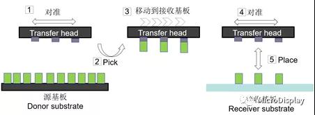
3. With the development of flexible and stretchable optoelectronic devices, display technology is gradually applied in wearable and bioelectronic field, which requires Micro LED grown on source substrate to be transferred to flexible substrate. On the other hand, due to the size of the wafer, it is necessary to transfer the Micro LED separated from the substrate from the source substrate or intermediate carrier substrate to the display panel. Chip pick-and-place is to place Micro LED on source substrate in target position by chip pick-and-place equipment with high precision and high speed, which is the key step to realize huge transfer. According to the different ways of implementation can be divided into accurate pickup, laser-induced transfer, self-assembly technology. 3.1 The correct pick-up technique generally completes the transfer process by transferring the device on the source Substrate (Donor Substrate) to the appropriate position and releasing it onto the receiving Substrate (Receive Substrate) , this process is shown in Fig. 5. The technique can be viewed as a process of interface competitive fracture, picking up when the force between the transfer head and the wafer is greater than the adhesion force between the wafer and the source substrate, when the interface adhesion between the receiving substrate and the chip is greater than the force between the transfer head and the chip, the release is realized, and the selectivity is realized by the pick head of the transfer device, and this mechanism in the field of flexible electronic transfer printing technology has a more in-depth study.

3.3 The concept of self-assembly, which usually refers to the spontaneous formation of ordered structures from basic structural units (molecules, nanomaterials, materials of Micron or larger scale) , was born at the end of the last century, and has been applied in many fields, such as optoelectronic materials, biomaterials, medical materials, etc. . The defect level of self-assembled products is low because the process of self-assembly is spontaneous, that is to say, the components are assembled according to the structure and combination way. In addition, the equipment needed for self-assembly technology is relatively cheap and the self-assembly process is relatively fast, because the self-assembly process itself is the self-assembly of the components into products. At present, Self-assembly technology is mainly divided into Molecular Self-assembly and Directed Self-assembly, which are composed of Molecular Self-assembly and Molecular Molecular Self-assembly Self-assembly. Molecular self-assembly, directed self assembly as shown in figure 8, is based on fluid, electromagnetic field, and directed self assembly, which was developed under the situation that the traditional technology can not meet the needs completely and the Molecular self-assembly technology is not mature. The methods include directed self assembly based on surface tension, directed self assembly driven by capillary force, and mixed 3D directed self assembly based on size matching, surface tension, and sequential self assembly. As a parallel manufacturing technology, self-assembly technology has been proposed as a fluid force.
At present, magnetic self-assembly and fluid self-assembly are two representative self-assembly technologies. Magnetic Self Assembly is a technique developed by Self Array, which uses magnets, vibrations and levitation to assemble leds into arrays. First, the LEDS are coated with a pyrolytic graphite film and placed on a magnetic platform, led by a magnetic field, the LEDS are quickly aligned to position. In this way, the magnetic platform needs to be dealt with first, so that the magnetic platform can have a well designed array distribution, and the segmented LED can be quickly positioned in the presence of a magnetic field, and then it will pass through an intermediate medium like PDMS, onto the target substrate. Fluid self-assembly technology is eLux companies use the role of fluid, so that LED into a good special structure, to achieve the effect of self-assembly. eLux applied for the patent in 2017. Any new system that relies on self-assembly can either tolerate its defects or fix them. The defect problem of self-assembly technology is always the key problem of self-assembly technology, how to realize the reversible, self-regulating or on-line monitoring of self-assembly process can reduce or avoid the defects of self-assembly, such as the correct synthesis, size effect, kinetics and mechanism, and characterization and control of self-assembly precursors, these are the key to the future development of self-assembly technology. 4. Based on the development background of modern display technology, this paper analyzes the development potential of Micro LED technology, and summarizes the advantages of Micro LED display technology. The preparation process of Micro LED display is briefly described. However, due to the large number of μLED miniaturization and full-color RGB μLED, it is difficult to realize the transfer with high precision and high yield using the existing transfer technology under the condition of considerable cost-benefit, it makes mass transfer become the key bottleneck technology that restricts its commercialization.
At present, a variety of technologies have been developed for mass transfer. Although these technologies are based on different principles, they all require the separation of the wafers from the source growth substrates and the selective placement of the wafers on the target substrates in some manner. The substrate separation is to process the source substrate in bulk by mechanical stress, chemical corrosion or laser, so as to facilitate the follow-up process. Relatively speaking, because of the complexity of mechanical stripping etching and the non-uniformity of etching degree, the selective picking force must be adjusted according to the fracture characteristics of the single etching structure, and the selectivity is poor The chemical stripping is affected by reaction rate, and the chemical solution drying step is added in the later stage, and the process time is longer. The laser stripping technology can realize the high efficiency stripping, and is more convenient for the following selective stripping process, however, the problem of thermal damage to Gan film still needs to be solved.
Chip pick-and-place process is an important part of mass transfer technology. From the point of view of process, how to pick and place chips in high precision and selective batch is the core of each technology school. For precision pick-up technology, based on the Johannes Diderik van der Waals force, electrostatic force, electromagnetic force and other mechanical principles of pick-up and placement of the chip, through the transfer head to meet the selective operation, the amount of transfer depends on the size of the transfer head, but most of the technology has special requirements on the chip, such as the electromagnetic force transfer requires the inclusion of magnetic materials such as iron, nickel, etc. , microstamp transfer technology needs a weak connection structure between the chip and the substrate, which will influence the luminescent properties of the chip. Laser-driven transfer technology is based on the interaction mechanism between laser and material, which produces the force of transfer wafer by ablation or direct release, and realizes selectivity by means of mask, spot focusing array, etc. , compared with other technologies, laser has advantages in repairing, it can melt the bad points, and it has a great effect on improving the yield, but laser transfer can satisfy the high-speed and selective transfer, but the transfer accuracy is affected by many factors, laser parameters (such as laser energy density, pulse frequency, spot size, etc.) and geometry parameters of transfer device (such as plate spacing, chip spacing) need to be studied. Self-assembly technology can always achieve the correct position and assembly in the process of fluid flow, but the selectivity is poor, and the subsequent defect repair will be difficult.
In addition to selectivity and precision, transfer rate is also a key parameter to determine the practicability of different transfer technologies in order to improve economic and time efficiency. In mainstream technologies such as laser-driven, self-assembly, precision pick-up technology for elastomeric seals and roll-to-roll stamping, fluid assembly exhibits the fastest transfer rate -- 50 million chips per hour, the transfer rate of roll-to-roll printing is 36 million chips per hour, and the transfer rate of elastomer seal is 1 million chips per hour. From the transfer rate, the fluid assembly technology can provide good transfer performance, but the development of this technology is still in progress. Relatively speaking, the transfer rate of fluid assembly technology is high, but because of the difficulty of fluid force control technology, the probability of success is lower than other technologies, and the realization is more difficult; Roller transfer printing and micro-seal transfer technology are easy and have high transfer rate, but the selectivity is poor and the later overhaul is not easy to realize, which leads to low guarantee of yield, the transfer rate is greatly reduced, but the selectivity is relatively good and the yield is high. Because of its fast transfer speed, high reliability and good selectivity, laser-assisted technology can be applied to transfer any size of panel, and has a very high technical advantage in the future huge transfer technology.
As a whole, Micro LED display technology is still in its initial stage, but it has not been commercialized because of the bottleneck of huge transfer. There are two directions for its future application, one is the direction of small size, ultra-high resolution, and the other is the direction of large-scale giant TV. For Wafer Transfer, small size applications pay more attention to transfer accuracy in order to ensure ultra-high resolution display, and require lower assembly rate than large size applications, while larger size applications require the opposite, the larger display area means more chips need to be transferred, which means more attention is paid to assembly speed and cost. Generally speaking, small-size display applications such as wearable watches are easy to be implemented in Micro LED display because of the small amount of transfer and relatively low difficulty But the decisive factor of medium and large scale application such as TV is cost, that is to say, the technology needs to break through at present, and the possibility of commercialization is low.
