

Tel: +86-755-23016560
Contact : Mr. zhao
Mobile : +86 139 2573 3686
Fax: +86-755-23016560
E-mail:sales@bestsoon-china.com
website:en.bestsoon-china.com
Address : 2202, 23rd Floor, Jinhao Building, No. 109, Fuyong Section, Guangshen Road, Fenghuang Community, Fuyong Street, Bao'an District, Shenzhen
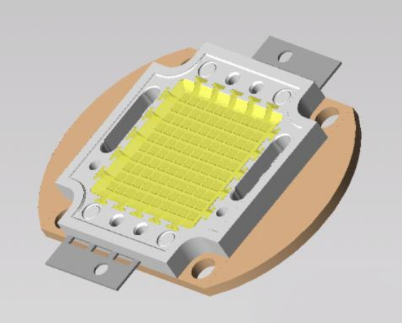
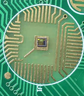
What is COB? Its full name is chip-on-board, that is, chip-on-board packaging. It is a new packaging method that is different from SMD surface-mount packaging technology. Specifically, the bare chip is adhered to the PCB with conductive or non-conductive glue, and then the lead is carried out. The electrical connection is realized by bonding, and the chip and the bonding wire are encapsulated with glue.
This packaging method does not require packaging, but integrates upstream and downstream companies. The production from packaging to LED display unit modules or displays is completed in one factory, which integrates and simplifies the production processes of packaging companies and display manufacturers. The production process is easier to organize and control, the product point spacing can be smaller, the reliability is doubled, and the cost is closer to civilians.
It was first applied in lighting, and this application has also become a trend. It is understood that COB-encapsulated bulb lamps have occupied about 40% of the LED bulb market.
With the gradual maturity of the LED application market, users have higher and higher requirements for product stability and reliability, especially under the same conditions, requiring products to achieve better energy efficiency indicators, lower power consumption, and more competition Strong product prices. Based on this, compared with traditional LEDSMD chip packaging and high-power packaging, chip-on-board (COB) integrated packaging technology directly encapsulates multiple LED chips on a metal-based printed circuit board, as a lighting module directly through the substrate Heat dissipation can not only reduce the manufacturing process and cost of the bracket, but also has the heat dissipation advantage of reducing thermal resistance, so it has become a packaging method recommended by lighting companies.
In addition to good heat dissipation performance and low cost, the COB light source can also be customized. However, technically, COB packaging still has shortcomings such as light attenuation, short life, and poor reliability. If it can be solved, it will be one of the leading directions for future packaging development.
The application of COB in lighting has become a trend and trend. So, can this packaging technology be applied to displays? In terms of packaging methods, some companies have made new attempts, and this attempt has also been verified, and has been promoted and used in the market. At the same time, it has also attracted widespread attention from people in the industry. So, why does COB display get everyone's attention? There must be a reason for this.
1. Analysis of the advantages and disadvantages of COB packaging
The application of COB packaging has been used in the field of lighting for many years, and it has many advantages in all aspects, so it has been favored by many lighting companies. Then, what kind of sparks will COB packaging technology apply to the display screen? Will there be some levels of non-compliance? Let's analyze the advantages and disadvantages of COB packaging. It is understood that the application of COB packaging technology to the display has an incomparable advantage over traditional packaging technology.
1. Ultra-light and thin: According to the actual needs of customers, PCB boards with thickness from 0.4 to 1.2mm can be used to reduce the weight at least to 1/3 of the original traditional products, which can significantly reduce the structure, transportation and engineering costs for customers.
2. Anti-collision and compression: COB products directly encapsulate the LED chip in the concave lamp position on the PCB board, and then encapsulate and cure it with epoxy resin. The surface of the lamp point is convex into a spherical surface, which is smooth and hard, resistant to impact and abrasion.
3. Large viewing angle: The COB package adopts shallow well spherical light emitting, the viewing angle is greater than 175 degrees, close to 180 degrees, and has a better optical diffuse color effect.
4. Flexibility: Flexibility is a unique feature of COB packaging. PCB bending will not cause damage to the packaged LED chips. Therefore, the use of COB modules can easily produce LED curved screens, circular screens, and wave-shaped screens. . It is an ideal base material for personalized screens in bars and nightclubs. It can be seamlessly spliced, the production structure is simple, and the price is far lower than the LED special-shaped screen made of flexible circuit boards and traditional display modules.
5. Strong heat dissipation ability: COB products encapsulate the lamp on the PCB board, and quickly transfer the heat of the wick through the copper foil on the PCB board. Moreover, the thickness of the copper foil of the PCB board has strict process requirements, plus the immersion gold process. Hardly cause serious light attenuation. Therefore, the lamp is rarely dead, and the life span is greatly extended.
6. Wear-resistant and easy to clean: the surface of the lamp point is convex into a spherical surface, smooth and hard, resistant to impact and wear; if there is a bad point, it can be repaired point by point; there is no mask, and it can be cleaned with water or cloth when there is dust.
7. All-weather excellent characteristics: triple protection treatment, waterproof, moisture, corrosion, dust, static electricity, oxidation, ultraviolet effect is outstanding; meet all-weather working conditions, the temperature difference environment of minus 30 degrees to above 80 degrees can still be used normally.
Speaking of, the advantages of COB display packaging are really many, especially when compared with the traditional packaging form, the contrast effect is more obvious. Since there are many advantages, why hasn't it been used on a large scale in the early development of LED display? Where are the shortcomings of COB packaging? Hu Zhijun, deputy general manager of Shenzhen Weiqiaoshun Optoelectronics Co., Ltd. said: “One of the disadvantages of COB packaging is that the ink color of the screen is not easy to control, which is the problem of inconsistent ink color on the surface when the lamp is not on.” Shenzhen Aolaida Technology Yang Rui, the marketing director of the Co., Ltd., also said frankly: "The flaw of COB display packaging lies in the lack of consistency on the surface. If this problem is not solved, it will be difficult to get customers' approval."
2. Interpretation of COB packaging process
COB packaging technology is again classified as a package-free or package-saving mode, but this packaging method does not eliminate the packaging process, but eliminates the packaging process. Compared with the placement process, the COB packaging process needs to be saved. Going to a few steps saves time and craftsmanship to a certain extent, and also saves costs to a certain extent. The production process of SMD needs to go through such links as die bonding, wire bonding, dispensing, baking, stamping, color separation, braiding, and patching. The COB process is simplified on this basis. First, the IC is attached to the circuit board. It is then solidified, wire-bonded, tested, glued and baked to become a finished product.
From the perspective of the production process alone, several steps are omitted. According to industry insiders, in this way, a large part of the cost can be saved. It is worth noting that the COB package does not require reflow soldering, which has become one of the advantages of COB.
Aureida Marketing Director Yang Rui said that the conventional packaging is to put the lamp beads on the PCB board for welding. As the lamp becomes denser, the lamp pin will become smaller and smaller, so the precision of the welding will be higher. How many lamps are there in a square, and a lamp has four pins, then a square will have many solder joints. At this time, the requirements for solder joints are very high, so the solution is to reduce the solder joints. Small solders have poor stability, and they may fall off if they are touched casually. This is an unavoidable problem for SMD; COB packaging eliminates the need for spectroscopy, color separation, drying and other processes. The most critical difference is to remove the solder. In the process of SMD soldering, it is extremely difficult to control the temperature. If the temperature is too high, the lamp will be damaged, and if the temperature is too low, the solder will not completely melt. It is easy to cause phenomena such as false welding and false welding, which is a big challenge to the stability of the lamp beads. COB does not have this process, so the stability will be greatly improved.
There are many processing techniques for traditional LED display screens. Especially in the process of reflow soldering, the expansion coefficients of the SMD lamp bead bracket and epoxy resin are different under high temperature conditions, which can easily cause the bracket and the epoxy resin encapsulation shell to fall off. Cracks, the phenomenon of dead lights gradually appeared in the later use, resulting in a higher defect rate. The reason why the COB display is more stable is that there is no reflow soldering and pasting lamp in the processing technology. Even if there is a later reflow soldering and pasting IC process, the diode chip has been encapsulated and cured with epoxy resin to protect it, and soldering is avoided The problem of gaps between the lamp bead bracket and the epoxy resin caused by high-temperature soldering in the machine.
3, the challenges faced by COB packaging
The emergence of a new product, a new technology and a new process will never go smoothly. It has to be tested and tried continuously in the R&D and production process before the problem is found and the right medicine can be solved in real time. The emergence of every problem is a process for R&D personnel to tackle key problems. In this process, it is full of hardships, but at the same time it is accompanied by achievements and satisfaction. The development of all new things is perfected bit by bit, and is approaching success step by step. But for now, the development of COB packaging technology cannot be called mature. After all, it will take time for the development of new things to mature. At this stage, COB packaging technology is still facing some challenges, and these challenges are gradually improved in the continuous efforts of enterprises.
It is understood that at present, there are still three challenges in COB packaging technology.
1. One pass rate of the packaging process
COB packaging method due to its characteristics, COB packaging is to be on a large board, this board has a maximum of 1024 lights, if the SMD seals a light, you only need to replace one, but the COB package is 1024 After the encapsulation of the lamps is completed, a test must be performed. After all the lamps are confirmed to have no problems, the sealing can be performed. How to ensure that the entire board of 1024 lights is completely intact, one pass rate is a very big challenge.
2. One pass rate of finished products
For COB products, the lamp is sealed first. After the lamp is sealed, the IC driver must undergo a reflow soldering process. How to ensure that the high temperature of 240 degrees in the furnace will not cause damage to the lamp when the lamp surface is reflowed. This is another big challenge. Compared with SMD, COB saves the reflow soldering process of the lamp surface, but the device surface needs to be reflow soldered just like SMD. That is to say, SMD has to be reflow soldered twice. However, when SMD is reflowed, the temperature in the furnace will cause two kinds of damage to the lamp surface. One is the wire bonding. If the temperature is too high, it will expand rapidly and cause the filament to break. The second is The heat in the furnace is quickly transferred to the wick through the 4 pins of the bracket, and small fragmentation damage may be caused on the wick. This damage is very fatal and is often difficult to detect, including the aging test, but it is also difficult to detect. This kind of tiny damage to the crystal, the tiny cracks, after a period of time
Use, this kind of malpractice will be highlighted, and then cause the lamp to fail. The COB is to ensure that when the lamp surface is reflowed, the high temperature in the furnace will not cause damage to it and ensure the yield. This is also a very important level.
3. Repair of the whole lamp
For the maintenance of COB lights, professional repairs and maintenance are required. One problem with single lamp maintenance is that after repairing, a circle will appear around the lamp. If a lamp is repaired, the surrounding circle will be smoked by the welding torch, and the maintenance is more difficult.
When there are challenges, it is necessary to find out the corresponding solutions. At present, for the problems encountered in the packaging and maintenance of COB packaging, companies have come up with corresponding solutions. For example, when the lamp surface is reflow soldered, certain solutions are used. The lamp surface is protected in this way to reduce damage; point-by-point correction technology is used in the maintenance process to ensure the consistency between the lamp beads.
4, the development trend of COB packaging
One advantage of COB packaging is that it can be packaged directly on the PCB without being restricted by lamp beads. Therefore, the point pitch is not scientific for COB. In theory, it is very easy for COB packaging to achieve high density. . To borrow a word from industry insiders, COB packaging is tailor-made for small pitches.
Aureida Marketing Director Yang Rui said, "COB does not follow the conventional screen route, so the products made will be meaningless. COB is mainly used in small-pitch displays. At present, small-pitch displays are widely used in the security field, so One of the main application areas of COB displays is security."
Hu Zhijun, deputy general manager of Wei Qiaoshun Optoelectronics Co., Ltd. also expressed the same view, “SMD needs to solve the problem of soldering feet. A lamp bead has four soldering feet. Then with the higher density of the display screen, the use of The number of lamp beads will be more and the solder feet will become denser. If this problem is not solved, miniaturization is a very big challenge for surface mounts. COB skips this part of the bracket, and millions of solder joints All of the problems are left behind, so miniaturization is easier."
"One of the characteristics of COB packaging is that it can well solve the problem of outdoor protection. Wei Qiaoshun has adopted a strategy of "rural surrounding the city" and first develops small outdoor spacing. For COB, even if it reaches P3, P2.5, P1.8 is easy to achieve, so Wei Qiaoshun intends to seize the time and seize the opportunity to break through the small outdoor space first, and use the advantages of high reliability to infiltrate the field of small indoor space." Hu Zhijun described the future development blueprint in this way.
"We believe that COB has a very good development prospect, because the reliability of COB products is much higher than that of surface mount products. This is one point; the second point is that as the dot density is smaller, the cost of COB products is lower, and they are closer to civilians. These are two very important characteristics. They are enough to support COB to a better future.
"For COB, it is not limited by lamp beads. It can be made easily below 1.0, but the products made will lose its meaning and value without the market. COB display is the hope of the future, but It will take some time for this road to go smoothly. Because more efforts are needed to solve the consistency problem. COB is a very good development trend. Because the prices of the two are similar, but The cost of COB should be about 15% lower. One is the process problem, which requires several process flows to be omitted, and the other is that it is easier to achieve mass production."
 Company Name :
Shenzhen Bestsoon ElectronicTechnology Co., Ltd.
 Contact number:+86-755-23016560
 Tel:+86 139 2573 3686 ( Zhao)
+86 137 9879 5391 ( Huang)
+86 133 0291 7860 (Yang )
 Fax: +86-755-23016560
 E-mail:sales@bestsoon-china.com
 Address:2202, south side, 23rd floor, Jinhao building, Fenghuang Community, Fuyong Street, Bao an district, Shenzhen